
Home » Posts tagged '5 stage pipeline'
Tag Archives: 5 stage pipeline
Design and Implementation of five stage pipeline
3.1 Introduction
In computer hardware some RISC CPU are MIPS, SPARC, Motorola 88000 and later DLX. Each of these classic scalar RISC designs fetched and attempted to execute one instruction per cycle. The main common concept of each design was a five-stage execution instruction pipeline. During operation, each pipeline stage would work on one instruction at a time. MIPS (Microprocessor without Interlocked Pipeline Stages) is a reduced instruction set computer (RISC) instruction set architecture (ISA) developed by MIPS Technologies (formerly MIPS Computer Systems, Inc.). The early MIPS architectures were 32-bit, with 64-bit versions added later. This part describes the 5 stage pipeline architecture and also discusses the functionality of each stage. This section is further divided into 4 subsections. Section 3.2 analyses the given MIPS model and its implementation, 3.3 describes the simulation using the trace files, 3.4 does a comparison between the 3 stage pipeline and the 5 stage pipeline and finally we end in section 3.5 by concluding.
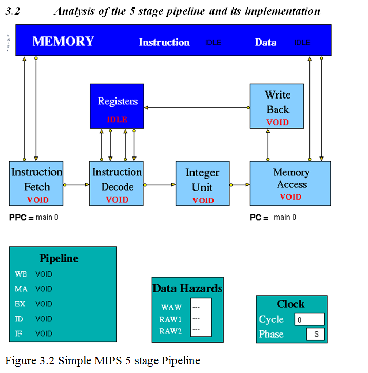
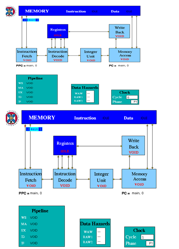
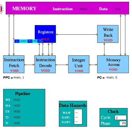
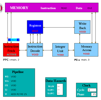
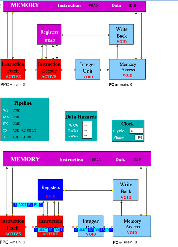
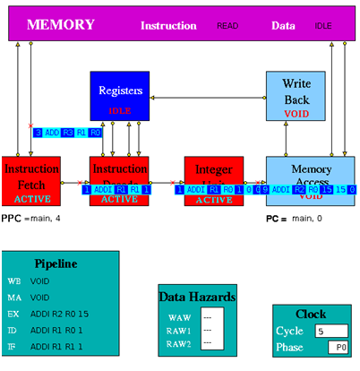
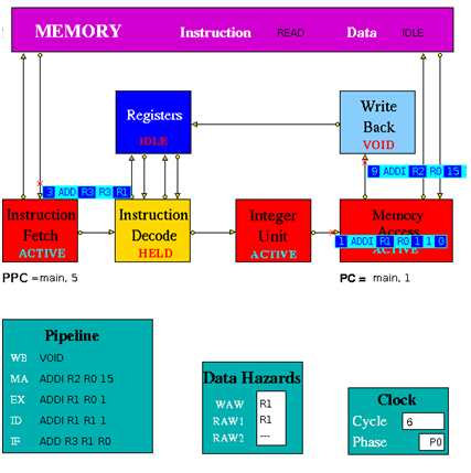
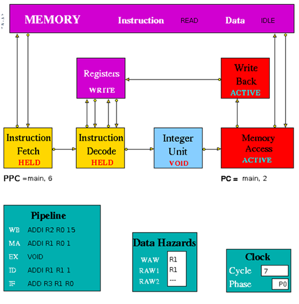
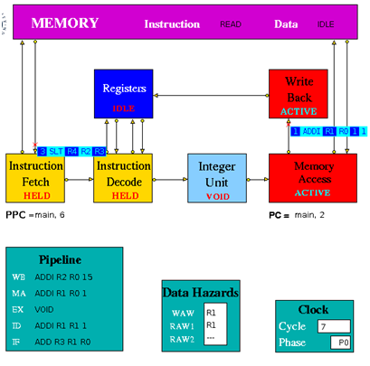
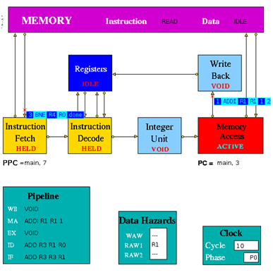
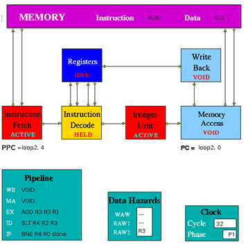
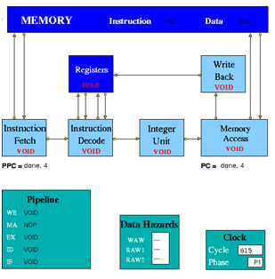
Figure 3.2 is an implementation of simple pipeline MIPS architecture. It is a 5 stage pipeline. The Integer Unit is used for both data and address arithmetic, so load/store instructions are processed by the Integer Unit before sending it to the Memory Access Unit and then to Memory. It also executes the additions required for integer test and relative branch instructions, so the Memory Access Unit also executes branches. The Integer Unit receives its operands from the Instruction Decode Unit, which is closely coupled to the Registers. These consist of 32 Integer Registers. The results from both arithmetic/logic and load instructions are returned to the Registers by the Write Back Unit. The model uses the Clock entity which sends (untraced) clock signal packets to the other units and each Unit sends a DONE signal back to clock when it has completed its actions. Each clock signal is generated when all units are done, thus ensuring that the architecture acts as a synchronous system. There are two signals in each clock period (corresponding to rising and falling edges of a square wave in hardware) denoting the start of phases 0 and 1 of the period. Entities compute in phase 0 and communicate in phase 1.
Instruction Fetch: The Instruction Fetch Unit accesses the Memory for instructions using the address in a Pre-fetch Program Counter (PPC). PPC is initially set equal to 0 (as is the PC register in the Memory Access Unit). If the IF Unit decodes a branch, it enters Held mode, waiting for the branch to be executed by the Memory Access Unit. If the branch results in a change to PC (i.e. other than by a normal increment) the pre-fetched instruction waiting to be copied into the Input Buffer has to be discarded. Because of the pre-fetching, there has to be at least one extra instruction (e.g. NOP 0) at the end of a program. In the phase 0 of the clock cycle first a normal PPC update is done. If there is a packet from the MA unit then update the PPC. If IF is not held up by a branch or external conditions then check for reply from memory and copy packet received into input register. At a pipeline clear, ClearValid flag is set which says all instructions are invalid until one is returned with bit 28 set indicating first of new sequence. This bit is set with first request to memory after a clear and resets ClearValid flag when it returns. If it is a valid instruction then decode the input register content to look for branches and set the variable Branch to true and decode absolute jumps to stop pre-fetching. If the instruction issued is a valid instruction, and it is not a ‘filler’ instruction (i.e. NOP / VOID), increment the global function. If PPC has been initialised from PC and if there are none or one memory requests outstanding then access memory for next instruction and increment Pre-fetch Program Counter. After these set the state and send the packets to the pipeline display i.e. pipe_disp. Copy the input register into the output packet and in phase 1 send the output to the instruction decode. If IFHold is set, do not send any instructions to Instruction Decode unless ClearValid is set (after a branch) and instruction in ID is not a Delay Slot instruction.
Instruction Decode: The Instruction Decode Unit receives instruction packets from the Instruction Fetch Unit and sends instruction/operand packets to the Integer Unit. Before accessing operands from the Registers, it checks for data hazards. If a hazard is detected, the Unit enters the Held state and the instruction remains in the Instruction Decode Unit until the next clock, when the checks are repeated.
In phase 0 of the clock cycle if IDHold or Hazard is set then no packet might have been sent to this unit and so no packets must be sent to execution units. If ID Hold is set, current instruction must not be processed. At a pipeline clear, ClearValid flag is set which says all instructions must be set invalid until one arrives with bit 28 set indicating first of new sequence. This bit resets ClearValid then send packet to the pipeline display (pipe_disp) to allow write by WB unit. Then check for double cycle orders and check for the hazards i.e. check if WAW is clear and check if RAW is clear. Then if ALU or store function is there then check for the RAW2 is clear or not. Then check for structural and control hazards i.e. whether execution units can accept instruction or not. For this there needs to be a temporary packet, which is non-valid if instruction in ID_Input_Reg is non-valid or is set non-valid if instruction can’t be sent to Execution Unit because of RAW or WAW, so that SB can insert a 0-latency instruction into latency queue and then update the scoreboard display. If the instruction is valid and if any hazard is detected then set my_state to held, and if the instruction is valid and there is no hazards detected then assemble the output. Copy the instruction and status into output register. Then in phase 1 of the clock cycle send the packet to the relevant execution unit.
Instruction Execute (Integer Unit in the figure 3.2): The Integer Unit receives instruction/operand packets from the Instruction Decode Unit and sends instruction/operand packets to the Memory Access Unit. In the current model the result of the arithmetic/logic instruction is computed using native-mode operations of the simulation execution platform. Each contains a pipeline with length equal to its latency value. Except in the case of the Integer Unit, this value is a parameter of the parent Execution Unit, so the code is designed to deal with any value (>=1) and can be common to all units. The Integer Unit executes instructions ADD, ADDI, SUB, SUBI,AND, ANDI, OR, ORI, XOR XORI, NOR, SSL, SRL, SRA, SLLV, SRLV, SRAV and is involved in the execution of LB, LBU, LH, LHU, LW, SW, SF, BNEZ, J, TRAP. In the output, the data2 field is only used for store instructions. The compare instructions (SLT, SLTI, SLTU, SLTUI) set the output data field to 1, if the condition is satisfied, and to 0 if not. In phase 0 of the clock cycle if the Hold is false then move instruction/operand packets through pipeline registers. If Stage 0 contains a valid instruction, compute Result and copy into first Pipeline stage output register (Pipeline[0]). Then set the state and send the packet to the pipeline display. In phase 1 of the clock cycle ,if not held up send the output to MA unit.
Memory Access Unit: The Memory Access Unit receives instruction packets from the Integer unit. Each packet contains two data fields in addition to the instruction and status fields. Arithmetic instruction packets contain the data to be sent to the registers via the Write Back Unit in the data1 field. Load instruction packets contain a memory address in the data1 field which is sent to the Memory Unit. The data returned from the Memory is passed to the Write Back Unit. Store instruction packets contain a memory address in the data1 field and the data to be sent to Memory in the data2 field. Branch instruction packets contain the new PC address or the offset in the instruction field of the packet. Conditions are evaluated in the relevant Execution Unit and carried through as bits in the Status field of the packet. When the appropriate change has been made to the Program Counter, an untraced packet is sent to the Instruction Fetch Unit to unlock the Held condition in that Unit and to update the Pre-fetch Program Counter. This unit receives all instructions that have completed execution. Arithmetic instruction packets contain the data to be sent to the registers via the Write Back Unit in the data1 field. Branch instruction packets contain the new PC address or the offset in the instruction field of the packet. Conditions are evaluated in the relevant execution unit and carried through as bits in the Status field of the packet. If a control transfer occurs an untraced packet is sent to the Instruction Fetch Unit to update. In phase 0 of the clock cycle unless MA is held up waiting for a reply from memory, check for valid packet from execution units. Then copy valid packet to MA_Input_Reg. In this unit always send the packet to the Pipeline Display even when held. Then the input instruction processing can be done if it is Arithmetic instructions then forward to Write Back Unit, if it is Load instructions then send Read access to Memory and set waiting flag, if it is Store instructions send Write access to Memory and set waiting flag and if it is Branch operations then execute. If MAHold = 1, look for packet from memory, for STORE orders, then this is an acknowledgement and for LOAD orders, the packet contains data which must be processed. In phase 1 of the clock cycle if Forward = 1, send the output to Write-Back unit. If Update_PPC is set, send PC value(s) to Instruction Fetch Unit.
Write Back: The Write Back Unit receives packets from the Memory Access Unit. Whenever a valid packet is received, the Write Back Unit constructs a Register Write Request packet and sends it to the Registers. The Registers have three ports, two for reading and one for writing. The Registers unit is not clocked and acts immediately on each packet it receives. To ensure that the simulation works correctly, there is a short delay in the Instruction Decode unit before it performs the WAW/RAW checks or reads the register values, i.e. a value being written in one clock cycle can also be read in that clock cycle.
3.3 Simulation using the trace files.
When first loaded, the model contains a program in its Instruction Memory which finds all prime numbers between 0 and 15. The Data Memory is initialised with the numbers 0 to 15. The program has two nested loops. The inner loop sets values in memory which are multiples of n (held in R1) to zero; n (initially set to 1) is incremented at the start of each iteration of the outer loop. The program ends when n reaches the limit of 15 set in R2. The non-zero numbers remaining in memory are prime numbers.
3.4 Simulation Analysis
To process the 17 instructions the 3 stage pipeline took 1024 clock cycles and total time taken is 20470ns .The 5 stage pipeline took 615 clock cycles and total time taken is 12310ns to execute 17 instructions.
The three stage pipeline took 315ns for the first instruction to complete all the pipeline stages and in 5 stage pipeline the same instruction took 150ns to complete all the stages of the pipeline.
3.5 Conclusion.
Pipelining doesn’t increase the performance of the processor. It increases the number of clock cycles it takes to execute a program. The performance benefit of pipelining comes from the fact that, because less number of the logic gates in the data path gets executed in a single cycle in a pipelined processor. Since the pipelined processor has a throughput of one instruction per cycle, the total number of instructions executed per unit time is higher in the pipelined processor, giving better performance. From section 3.4 it is clear that 5 stage pipeline is better than the 3 stage pipeline since to process 17 instructions the 5 stage pipeline took 12310ns of time and the 3 stage pipeline took 20470ns. So the percentage of improvement in 5 stage pipeline to that of 3 stage pipeline is approximately 40%.
Link to design and Implementation of three stage pipeline
References
____________________________________________________________________
[1] Hennessy,J. and Patterson,D. (2005) Computer Organization and Design:T H E H A R D W A R E / S O F T W A R E I N T E R F A C E,3rd edition,Morgan Kaufmann
[2] Hennessy,J. and Patterson,D. (2007) Computer Architecture: A Quantitative Approach, 4th edition, Morgan Kaufmann.
[3] Hesham,E.R. and Mostafa,A.(2005) ADVANCED COMPUTER ARCHITECTURE AND PARALLEL PROCESSING,John Wiley & Sons
[4] Smith,M., Johnson and Horowitz,M.A.(April 1989) “Limits on Multiple Instruction Issue“, Proceedings of the 3rd International Conference on Architectural Support for Programming Languages and Operating Systems.
[5] Princeton wordnet web [Online] Available from http://wordnetweb.princeton.edu/perl/webwn?s=Computer+Architecture&sub=Search+WordNet&o2=&o0=1&o8=1&o1=1&o7=&o5=&o9=&o6=&o3=&o4=&h=
Accesses:31 December 2012
Appendix A MIPS Instruction Sets
____________________________________________________________________
Load/Store Instructions
| Instruction | Description | Example | Result |
| LB | Load Byte | LB R3 1(R0) | Loads Byte from memory location 1 |
| LBU | Load Byte Unsigned | LBU R4 1(R0) | Loads Byte Unsigned from memory location 1 |
| SB | Store Byte | SB R1 1(R0) | Stores Byte in R1 into memory location 1 |
| LH | Load Halfword | LH R4 2(R0) | Loads Halfword from memory location 2 into R4 |
| LHU | Load Halfword Unsigned | LHU R4 2(R0) | Loads Halfword Unsigned from memory location 2 into R4 |
| LUI | Load Upper Immediate | LUI R1 124 | Load 124 in the the upper half of regester R1 |
| SH | Store Halfword | SH R5 6(R0) | Stores Halfword from R5 into memory loction 6 |
| LW | Load Word | LW R4 8(R0) | Loads Word from data memory loaction word 8 into R4 |
| SW | Store Word | SW R3 16(R0) | Stores Word in R3 into location 16 in data memory |
Arithmetic instructions
| Instruction | Description | Example | Result |
| ADDI | Add Immediate Word | ADDI R1 R2 -4 | Store R2 + -4 in R1 |
| ADDIU | Add Immediate Unsigned Word | ADDIU R1 R2 16 | Store R2 + 16 in R1 |
| ADD | Add Word | ADD R1 R2 R3 | Store R2 + R3 in R1 |
| ADDU | Add Word Unsigned | ADD R1 R2 R3 | Store R2 + R3 in R1 |
| SUB | Subtract Word | SUB R1 R2 R3 | Store R2 – R3 in R1 |
| SUBU | Subtract Word Unsigned | SUB R1 R2 R3 | Store R2 – R3 in R1 |
| SLT | Set on less than | SLT R1 R2 R3 | If R2 is less than R3 set R1 to be 1 else set it to 0 |
| SLTI | Set on less than Immediate | SLTI R1 R2 5 | If R2 is less than 5 then set R1 to 1 else set it to 0 |
| SLTU | Set on less than Unsigned | SLTU R1 R2 R3 | If the unsigned value of R2 is less than the unsigned value R3 set R1 to 1 else set it to 0 |
| SLTIU | Set on less than Immediate Unsigned | SLTIU R1 R2 6 | If the R2 is less than 6 (after sign extension)set R1 to 1else set it to 0 |
Logical Instructions
| Instruction | Description | Example | Result |
| AND | And | AND R1 R2 R3 | Stores result of R2 AND R3 into R1 |
| ANDI | And Immediate | ANDI R1 R1 19 | Stores the result of R1 AND 19 back into R1 |
| OR | Or | OR R1 R2 R3 | Stores result of R2 OR R3 into R1 |
| ORI | Or Immediate | ORI R1 R1 128 | Stores the result of R1 OR 128 back into R1 |
| XOR | Exclusive Or | XOR R1 R2 R3 | Stores result of R2 XOR R3 into R1 |
| XORI | Exclusive Or Immediate | XORI R1 R1 64 | Stores the result of R1 OR 64 back into R1 |
| NOR | Nor | NOR R1 R2 R3 | Stores result of R2 NOR R3 into R1 |
| SSL | Shift Word Left Logical | SSL R1 R2 4 | Shift R2 4 bits to the left and store in R1 |
| SRL | Shift Word Right Logical | SRL R1 R2 2 | Shift R2 2 bits to the right and store in R1 |
| SRA | Shift Word Right Arithmetic | SRA R3 R4 2 | Arithmrticaly shift R4 2 bits right and store in R3 |
| SLLV | Shift Word Left Logical Varable | SLLV R1 R2 R3 | Shift R2 left by R3 bits and store in R1 |
| SRLV | Shift Word Right Logical Varable | SRLV R1 R2 R3 | Shift R2 right by R3 bits and store in R1 |
| SRAV | Shift Word Right Arithmetic Varable | SRAV R1 R2 R3 | Shift R2 right arithemeticaly by R3 bits and store in R1 |
Jump Instructions
| Instruction | Description | Example | Result |
| J | Jump | J 8 | Jump to instruction 8 |
| JR | Jump Register | J R1 | Jump to the instruction number held in R1 |
Branch Instructions
| Instruction | Description | Example | Result |
| BEQ | Branch on equal | BEQ R1 R2 4 | Branch forward 4 instructions if R1 and R2 are equal |
| BNE | Branch on not equal | BNE R1 R2 8 | Branch forward 8 instructions if R1 and R2 are not equal |
| BLEZ | Branch on less than or equal to zero | BLEZ R2 -2 | Branch back 2 instructions if R2 is less than or equal to zero |
| BGTZ | Branch on greater than zero | BGTZ R2 -2 | Branch back 2 instructions if R2 is greater than zero |
| BLTZ | Branch on less than zero | BLTZ R2 3 | Branch forward 3 instructions if R2 is less than zero |
| BGEZ | Branch on greater than or equal to zero | BGTZ R2 5 | Branch forward 5 instructions if R2 is greater than or equal to zero |
| BLTZAL | Branch on less than zero and link | BLTZAL R2 3 | Branch forward 3 instructions if R2 is less than zero |
| BGEZAL | Branch on greater than or equal to zero and link | BGTZAL R2 5 | Branch forward 5 instructions if R2 is greater than or equal to zero and link |
Other Instructions
| Instruction | Description | Example | Result |
| BREAK | Breakpoint | BREAK | Halt |
| NOP | No Operation | NOP | No operation |
Appendix B Instructions File (MEMORY.instr_mem.mem)
____________________________________________________________________
ADDI R2 R0 15
ADDI R1 R0 1
loop1:
ADDI R1 R1 1
ADD R3 R1 R0
loop2:
ADD R3 R3 R1
SLT R4 R2 R3
BNE R4 R0 done
SLL R5 R3 2
J loop2
SW R0 0(R5)
done:
BNE R1 R2 loop1
NOP
BREAK
NOP
Appendix C Parameter File (mips_v1.1.params)
____________________________________________________________________
0 (branches_taken)
0 (branches_not_taken)
0 (memory_reads)
0 (memory_writes)
0 (instructions_issued)
10 20 1 (log_max_cycles)
CLOCK (clockName)
IDLE (INSTRUCTION)
IDLE (DATA)
2 8 1 (d_accesstime)
1 (i_accesstime)
65536 (I_Mem_Size)
65536 (D_Mem_Size)
128 (NoOfElements)
64 (NoOfElements)
32 (NoOfElements)
CLOCK (clockName)
main (label)
0 (offset)
CLOCK (clockName)
CLOCK (clockName)
main (label)
0 (offset)
— (WAW)
— (RAW1)
— (RAW2)
0 (cycle)
10.0 (period)
-1.0 (period1)
CLOCK (clockName) 0 (cycle)
